Download Zip ⏩ https://urloso.com/2uZupb
Shift Register Parallel In Serial Out in VHDL Code: A Step-by-Step Guide
If you are looking for a way to implement a shift register parallel in serial out (PIPO) in VHDL code, you have come to the right place. In this article, we will show you how to write a VHDL code for a PIPO shift register using D flip-flops, and explain how it works.
What is a Shift Register Parallel In Serial Out?
A shift register parallel in serial out is a type of shift register that can load data bits in parallel and shift them out serially. A shift register is a sequential logic circuit that can store and manipulate binary data. It consists of a chain of flip-flops that can transfer data from one flip-flop to another when a clock signal is applied.
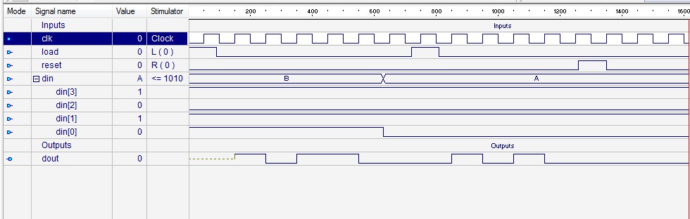
A PIPO shift register has n parallel inputs and one serial output. It can load n bits of data simultaneously into the flip-flops when a load signal is high, and then shift them out one by one from the least significant bit (LSB) to the most significant bit (MSB) when the load signal is low. The following figure shows the block diagram of a 4-bit PIPO shift register.

The PIPO shift register has four parallel inputs D3, D2, D1, and D0, and one serial output Q0. It also has a clock input CLK and a load input LD. When LD is high, the data bits at the parallel inputs are loaded into the flip-flops Q3, Q2, Q1, and Q0. When LD is low, the data bits are shifted to the right by one position at each clock cycle, and Q0 becomes the serial output.
How to Write a VHDL Code for a PIPO Shift Register?
To write a VHDL code for a PIPO shift register, we need to use a library and a package that provide the standard logic data types and operators. We also need to declare an entity that defines the inputs and outputs of the shift register, and an architecture that describes its behavior.
The library and package we need are ieee.std_logic_1164.all, which are included in most VHDL compilers. The entity declaration for a 4-bit PIPO shift register is as follows:
library ieee;

use ieee.std_logic_1164.all;
entity pipo is
generic (
n : integer := 4 -- number of bits
);
port (
clk : in std_logic; -- clock input
ld : in std_logic; -- load input
d : in std_logic_vector (n-1 downto 0); -- parallel inputs
q : out std_logic_vector (n-1 downto 0); -- parallel outputs
s_out : out std_logic -- serial output
);
end pipo;
The entity has five ports: clk, ld, d, q, and s_out. The clk and ld are single-bit inputs that control the clock and load signals. The d and q are n-bit vectors that represent the parallel inputs and outputs. The s_out is a single-bit output that represents the serial output.
The architecture declaration for a PIPO shift register is as follows:
architecture behavioral of pipo is

  signal temp_reg : std_logic_vector (n-1 downto 0); -- temporary register

begin

  process (clk)

  begin

    if rising_edge(clk) then -- on positive clock edge

      if ld = '1' then -- if load is high

        temp_reg <= d; -- load parallel inputs into temporary register

      else -- if load is low

        temp_reg <= temp_reg(n-2 downto 0) & '0'; -- shift temporary register to the right by one bit

      end if;

    end if;

  end process;
q <= temp_reg; -- assign temporary register to parallel outputs
s_out <= temp_reg(0); -- assign LSB of temporary register to serial output
end behavioral;
The architecture uses a signal called temp_reg to store the data bits in the flip-flops. The signal has the same size as the parallel inputs and outputs.
How to Implement a D Flip-Flop in VHDL Code?
A D flip-flop is a type of flip-flop that has a single data input D and a clock input CLK. The output Q of the D flip-flop follows the input D when the clock signal is high, and holds its value when the clock signal is low. The following figure shows the symbol and the truth table of a D flip-flop.
To implement a D flip-flop in VHDL code, we need to use a library and a package that provide the standard logic data types and operators. We also need to declare an entity that defines the inputs and outputs of the flip-flop, and an architecture that describes its behavior.
The library and package we need are ieee.std_logic_1164.all, which are included in most VHDL compilers. The entity declaration for a D flip-flop is as follows:
library ieee;

use ieee.std_logic_1164.all;
entity d_ff is
port (
clk : in std_logic; -- clock input
d : in std_logic; -- data input
q : out std_logic -- output
);
end d_ff;
The entity has three ports: clk, d, and q. The clk and d are single-bit inputs that control the clock and data signals. The q is a single-bit output that represents the output of the flip-flop.
The architecture declaration for a D flip-flop is as follows:
architecture behavioral of d_ff is

begin

  process (clk)

  begin

    if rising_edge(clk) then -- on positive clock edge

      q <= d; -- assign data input to output

    end if;

  end process;

end behavioral;
The architecture uses a process that is sensitive to the clk signal. The process checks if there is a rising edge on the clk signal, and if so, it assigns the value of the d input to the q output. This way, the output follows the input when the clock is high, and holds its value when the clock is low.
How to Use a PIPO Shift Register in a Calculator?
A PIPO shift register can be used in a calculator to store and manipulate binary data such as arithmetic operations, logical operations, encryption, etc. For example, suppose we want to perform a binary addition of two 4-bit numbers using a PIPO shift register. The following steps can be followed:
- Load the first 4-bit number into the parallel input pins of the PIPO shift register. For example, if the first number is 1010, then load D3 = 1, D2 = 0, D1 = 1, and D0 = 0.
- Apply a clock pulse to the shift register to transfer the parallel input to the parallel output pins. The output pins will have the same value as the input pins. For example, Q3 = 1, Q2 = 0, Q1 = 1, and Q0 = 0.
- Connect the parallel output pins of the PIPO shift register to the inputs of a 4-bit full adder circuit. The full adder circuit will perform the binary addition of the two numbers and produce a 4-bit sum and a carry bit.
- Load the second 4-bit number into the parallel input pins of another PIPO shift register. For example, if the second number is 0111, then load D3 = 0, D2 = 1, D1 = 1, and D0 = 1.
- Apply a clock pulse to the second shift register to transfer the parallel input to the parallel output pins. The output pins will have the same value as the input pins. For example, Q3 = 0, Q2 = 1, Q1 = 1, and Q0 = 1.
- Connect the parallel output pins of the second PIPO shift register to the other inputs of the 4-bit full adder circuit. The full adder circuit will perform the binary addition of the two numbers and produce a 4-bit sum and a carry bit.
- Read the sum and carry bits from the outputs of the full adder circuit. The sum bits will be the result of the binary addition and the carry bit will indicate if there is an overflow. For example, if the sum is 10001, then S3 = 1, S2 = 0, S1 = 0, S0 = 1, and C = 1.
The following figure shows a schematic diagram of using two PIPO shift registers and a 4-bit full adder circuit to perform a binary addition of two numbers.
How to Use a PIPO Shift Register for Encryption?
A PIPO shift register can be used for encryption by loading and shifting the data bits in a way that makes them unreadable by unauthorized parties. Encryption is the process of transforming data into a secret code that can only be deciphered by using a key. One of the methods of encryption is using a shift register as a stream cipher.
A stream cipher is a type of encryption that encrypts each bit of the data with a bit of a key stream. A key stream is a sequence of bits that are generated by an algorithm using a secret key. A shift register can be used to generate a key stream by loading an initial value (called seed) into the parallel input pins and then shifting the bits in a nonlinear fashion using feedback logic. The feedback logic can be implemented by using XOR gates, multiplexers, or other logic gates. The output pins of the shift register can be used as the key stream bits.
To encrypt the data, the key stream bits are combined with the data bits using XOR operations. The XOR operation produces a 1 if the inputs are different and a 0 if they are the same. The encrypted data is called ciphertext. To decrypt the ciphertext, the same key stream bits are combined with the ciphertext bits using XOR operations again. The XOR operation reverses the encryption and produces the original data bits.
The following figure shows an example of using a 4-bit PIPO shift register as a stream cipher.
In this example, the seed value is 1010 and the feedback logic is an XOR gate that takes the output of Q3 and Q1 as inputs. The shift register generates a key stream of 1010, 0101, 1011, 0110, 1101, 1110, 0111, and 1001. The data to be encrypted is 1100 and the ciphertext is 0110.
How to Write a VHDL Code for a PISO Shift Register?
A PISO shift register is a type of shift register that can load data bits in parallel and shift them out serially. A PISO shift register has n parallel inputs, one serial output, a clock input, and a load input. The load input controls whether the data bits are loaded from the parallel inputs or shifted from the previous stage.
To write a VHDL code for a PISO shift register, we need to use a library and a package that provide the standard logic data types and operators. We also need to declare an entity that defines the inputs and outputs of the shift register, and an architecture that describes its behavior.
The library and package we need are ieee.std_logic_1164.all, which are included in most VHDL compilers. The entity declaration for a 4-bit PISO shift register is as follows:
library ieee;

use ieee.std_logic_1164.all;
entity piso is
generic (
n : integer := 4 -- number of bits
);
port (
clk : in std_logic; -- clock input
ld : in std_logic; -- load input
d : in std_logic_vector (n-1 downto 0); -- parallel inputs
s_out : out std_logic -- serial output
);
end piso;
The entity has four ports: clk, ld, d, and s_out. The clk and ld are single-bit inputs that control the clock and load signals. The d is an n-bit vector that represents the parallel inputs. The s_out is a single-bit output that represents the serial output.
The architecture declaration for a PISO shift register is as follows:
architecture behavioral of piso is

  signal temp_reg : std_logic_vector (n-1 downto 0); -- temporary register

begin

  process (clk)

  begin

    if rising_edge(clk) then -- on positive clock edge

      if ld = '1' then -- if load is high

        temp_reg <= d; -- load parallel inputs into temporary register

      else -- if load is low

        temp_reg <= '0' & temp_reg (n-1 downto 1); -- shift temporary register to the right by one bit

      end if;

    end if;

  end process;
s_out <= temp_reg(0); -- assign LSB of temporary register to serial output
end behavioral;
The architecture uses a signal called temp_reg to store the data bits in the shift register. The signal has the same size as the parallel inputs. The process is sensitive to the clk signal and checks if there is a rising edge on it. If so, it checks the value of the ld signal. If ld is high, it loads the parallel inputs into the temp_reg signal. If ld is low, it shifts the temp_reg signal to the right by one bit and inserts a zero at the MSB position. The s_out output is assigned to the LSB of the temp_reg signal.
Conclusion
In this article, we have learned about the shift register parallel in serial out (PIPO) in VHDL code. We have seen how to implement a PIPO shift register using D flip-flops, and how to use it for various applications such as data storage, conversion, manipulation, and encryption. We have also learned how to write a VHDL code for a PISO shift register, which is another type of shift register that can load data bits in parallel and shift them out serially. We have also seen how to test and verify the functionality of the shift registers using testbenches.
Shift registers are useful sequential logic circuits that can be used for storing and transferring binary data. They can be categorized into different types based on the direction and mode of data movement. By choosing the right type of shift register and writing an efficient VHDL code, we can optimize the performance and resource utilization of our FPGA designs.
https://github.com/0inmenPgiga/run-on-arch-action/blob/master/.github/AutoCAD%202010%2064%20bit%20indir%20gezginler%20Mimarlar%20mhendisler%20ve%20tasarmclar%20iin%20profesyonel%20bir%20grafik%20ve%20tasarm%20arac.md
https://github.com/caigapei/pulumi/blob/master/coverage/HD%20Online%20Player%20(Passengers%20(English)%20720p%20Torrent%20Do)%20How%20to%20Download%20and%20Stream%20the%20Epic%20Space%20Adventure.md
https://github.com/swinurdeta/ehForwarderBot/blob/master/.github/workflows/Sonik%20Synth%202%20Authorization%20Code%2016%20The%20Secret%20to%20Creating%20Amazing%20Synth%20Sounds.md
https://github.com/turtaQimnu/sis/blob/master/.github/Beydavi%20Tefsiri%20Indir%20slam%20limleri%20ve%20Dier%20Alanlarda%20lmsz%20Bir%20Eser.md
https://github.com/1tincbiYcredchi/End-to-end-Autonomous-Driving/blob/main/assets/Max%20Payne%202%20Punisher%20Mod%20Tips%20and%20Tricks%20to%20Master%20the%20Game%20and%20Defeat%20the%20Enemies.md
https://github.com/pisiOmonsme/Book6_First-Course-in-Data-Science/blob/main/Book6_Ch14_Python_Codes/Highway%20Movie%20Download%20Kickass%20720p%20A%20Critically%20Acclaimed%20Masterpiece%20by%20Imtiaz%20Ali.md
https://github.com/tacesWliewa/god/blob/master/runner/The%20Negotiator%201998%20Br%20Rip%201080p%20Movie%20Torrents%20Find%20Out%20Where%20to%20Download%20the%20Full%20HD%20Film.md
https://github.com/motisneri/watermelon-extension/blob/dev/wm-paper/Sanda%20Marin%20Carte%20de%20bucate.pdf%20.md
https://github.com/buddmaWsuga/graphql-code-generator/blob/master/packages/Principles%20of%20Refrigeration%20Roy%20J%20Dossat%20PDF%20Download%20-%20A%20Comprehensive%20Guide%20to%20Refrigeration%20and%20Refrigerating%20Machinery.md
https://github.com/bellaFanyo/stable-diffusion-webui/blob/master/extensions/Xforce%20Keygen%20Collaboration%20For%20Revit%202012%2032bit%20Free%20Download%20How%20to%20Get%20the%20Most%20Out%20of%20Your%20Autodesk%20Products.md
86646a7979